The basis of all precision positioning and navigation is precision timing. Timing comes first. GPS Time is defined on the basis of a set of atomic clocks orbiting aboard the satellites and on the ground in monitoring stations; similarly for the other GNSS systems.
These atomic clocks are quite large, quite expensive, and the service they ultimately provide—the GNSS signals—is vulnerable to several types of interference and bias. If inexpensive, miniature atomic clocks could be placed aboard user equipment, many of these vulnerabilities could be obviated and precision greatly improved.
The U.S. Defense Advanced Research Projects Agency (DARPA) unveiled the first chip-scale atomic clock (CSAC) in 2003 and has steadily funded improvements to get the clocks even smaller, more precise, and less expensive. It recently announced three R&D projects well on their way to achieving these goals.
- The National Institute of Standards and Technology (NIST) collaborated with researchers at the California Institute of Technology, Stanford University, and Charles Stark Draper Laboratoriesto demonstrate an experimental optical atomic clock that is comprised of three small chips, supporting electronics and optics.
- Honeywell, in partnership with University of California, Santa Barbara, is developing precision atomic sensors based on a magneto-optic trap (MOT) produced by a three-dimensional arrangement of laser beams.
- NASA’s Jet Propulsion Laboratory (JPL), with researchers at SRI International, the University of California, Davis, and the University of Illinois Urbana-Champaign demonstrated an experimental atomic clock using an ion-based approach to atom cooling that relies on ionized mercury and ultraviolet lamps instead of lasers.
“Shrinking atomic clocks from large cesium beam tubes to chip-scale devices without eroding performance requires a rethinking of a number of critical components, including vacuum pumps and optical isolators as well as new approaches to component integration,” said Dr. John Burke, program manager for the Atomic Clock with Enhanced Stability (ACES) program in DARPA’s Microsystems Technology Office (MTO).
The projects may lead to new methods of atomic clock production at wafer scale. “The early progress made on ACES shows that there are viable options in development for doing this same thing without the massive engineering manpower or hefty costs associated with current approaches,” Burke added.
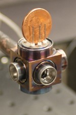
The first-generation CSACs developed by DARPA and NIST, now available commercially through Microsemi, have furnished CSAC proof of concept tehnology across DoD and civilian applications. Because of physics principles basic to their design, however, performance is limited by temperature sensitivity, long-term frequency aging, and turn-on to turn-on reproducibility, or retrace. The new developments funded by ACES may ultimately provide chip-scale atomic clocks with 1000x performance improvements.
Such precise timekeeping on portable platforms could greatly advance the robustness and ubiquity of 5G networks and many applications in navigation, financial transaction, distributed cloud, and defense. Ultimately, it is conceivable that they could lead to PNT alternatives that do not rely at all on GNSS signals from space.
The NIST-California Institute of Technology-Stanford-Draper Labsteam recently published a paper in the Optica scientific journal describing its work. The experimental optical atomic clock consists of three chips and supporting electronics and optics. While standard atom clocks use cesium atoms and operate at microwave frequencies, this one runs at higher frequencies and uses a laser to track oscillations of rubidium atoms confined in a 3-millimeter vapor cell atop silicon chip. Two frequency combs convert the rubidium atoms’ high-frequency optical ticks to lower microwave frequency for use in PNT applications. This produces a 50-fold increase in accuracy over current CSACs.
The Honeywell-University of California, Santa Barbarateam has precision atomic sensors using a magneto-optic trap (MOT) in place of bulky lenses and mirrors. The MOT employs a three-dimensional arrangement of laser beams crossing at a precise point, and enabled by an integrated photonic chip that guides light around an optical circuit. The process promises to adapt to batch fabrication of complex optical systems with reduced manufacturing cost.
The JPL-SRI International-UC Davis-University of Illinois collaboration focused on making its prototype resistant to temperature and environmental issues, a key factor affecting atomic clocks. An ion-based approach related to the Deep Space Atomic Clock (DSAC) [[link to https://insidegnss.com/deep-space-clock-could-blaze-trail-to-improved-gnss-accuracy/]]uses ionized mercury and ultraviolet lamps instead of lasers. This produced a temperature immunity roughly 100x better than current CSACs as well as less sensitivity to magnetic fields.